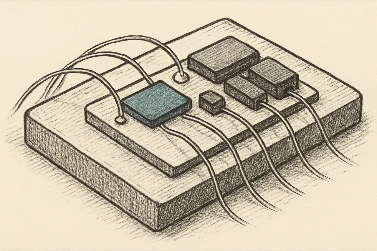
The Integrated Circuit Patent Jack Kilby Filed in 1959
Five months after Jack Kilby joined Texas Instruments, he had an idea while everyone else was on a company-wide vacation. The patent that resulted, US3138743, is the legal foundation of the entire modern semiconductor industry.
In July of 1958, Jack Kilby was a new hire at Texas Instruments. He had not accumulated enough vacation time to take the company-wide summer break, so when most of TI's research staff went home for two weeks, he stayed in an empty Dallas laboratory and worked alone.
The problem he was working on was the "tyranny of numbers" — the observation that electronic circuits had become limited not by the speed of their components but by the sheer impossibility of soldering enough of them together by hand. A single complex circuit might require thousands of resistors, capacitors, and transistors, each of them a separate physical part connected by a separate wire. As designs grew more ambitious, the assembly grew exponentially harder. The state of the art was running out of factory.
Kilby's idea, written into his lab notebook on July 24, 1958, was: what if all of the components were made out of the same material, and inside the same piece of it? If you fabricated the resistors and capacitors and transistors all from a single block of germanium, you could connect them with deposited metal lines on the surface, and the whole circuit would emerge from one piece of substrate. Kilby built a working prototype in early September. It was a phase-shift oscillator. It worked.
He filed for a patent on February 6, 1959. US3138743 was issued, after one of the longer examination periods in the patent office's history, on June 23, 1964.
The Noyce parallel
Six months after Kilby's notebook entry, Robert Noyce at Fairchild Semiconductor in California had a related but distinct idea. Where Kilby's prototype used hand-soldered gold wires across the surface of the germanium, Noyce realized that a thin layer of silicon dioxide — already part of the new "planar process" Fairchild was developing — could be used to deposit metal interconnects in a single fabrication step. Noyce filed his patent in July 1959. Both patents were eventually held to be valid; the legal fight between TI and Fairchild ran for the next decade and was finally resolved through a cross-licensing agreement that let both companies build on the foundational invention.
Kilby's design is the older one. Noyce's design is the one that became practical at scale. Modern chips owe both: the idea of the integrated circuit is Kilby's; the manufacturing process that made integration economically viable is Noyce's.
What it became
The world manufactured an estimated two trillion semiconductor chips in 2024. Every one of them descends from the principle described in US3138743 and its sibling at Fairchild. The personal computer, the internet, the modern smartphone, the GPS satellite, the implanted pacemaker, and the cruise missile all exist because two engineers in 1958 and 1959 figured out how to put more than one thing into a single piece of silicon at the same time.
Kilby received the Nobel Prize in Physics in 2000. Noyce, by then, had been dead for ten years and so was ineligible — Nobels are not awarded posthumously. The two had remained publicly cordial throughout their careers and had each insisted that the other deserved equal credit. The committee, in its citation, agreed.
See the original
The full text and figures of US3138743 are on patents.us.
Related stories
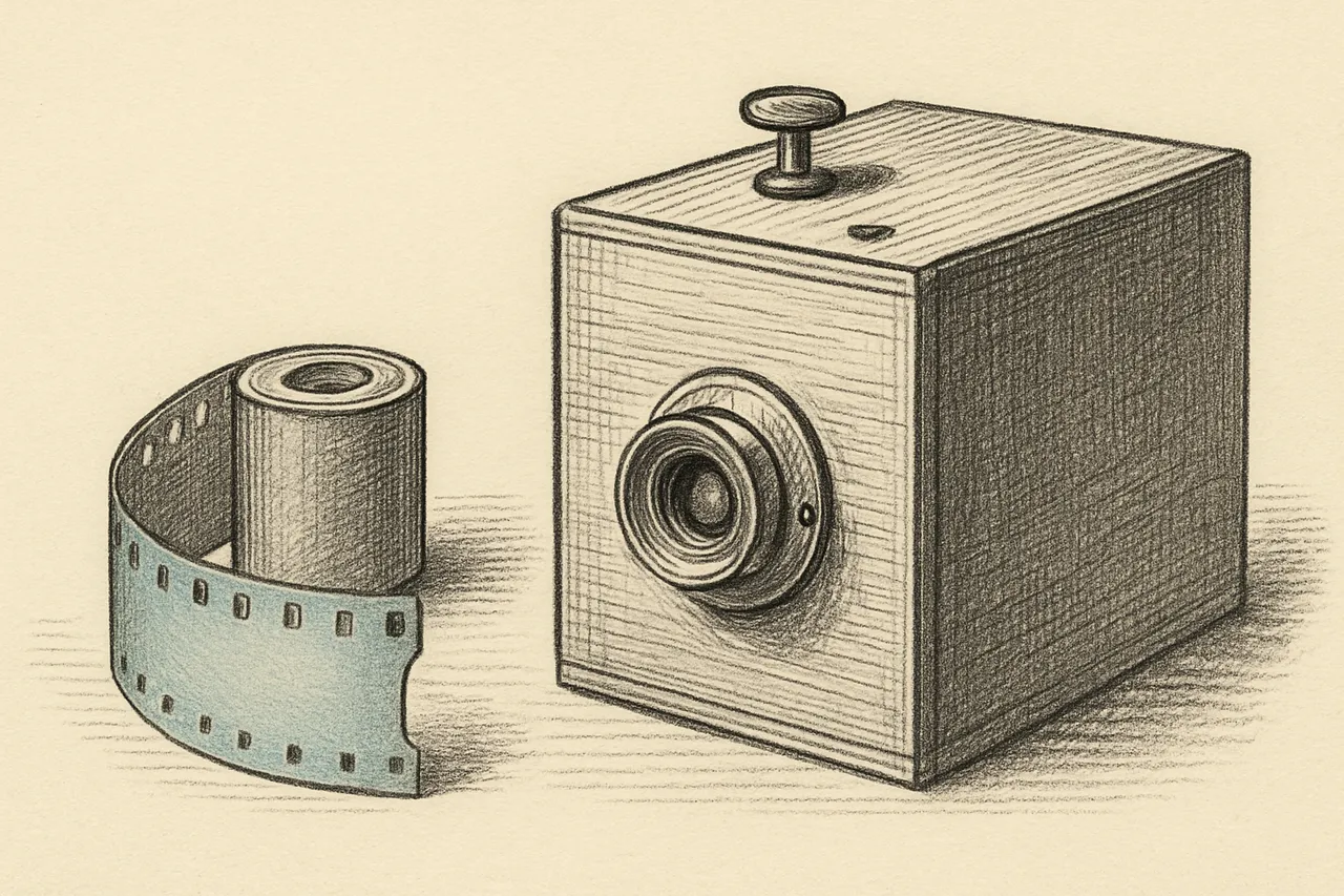
George Eastman Made Everyone a Photographer With Four Words: You Press the Button
Before 1888, photography meant glass plates, chemicals, and expertise. Eastman's roll-film box camera came pre-loaded, took a hundred pictures, and was mailed back to the factory for developing. The slogan said the rest: 'You press the button, we do the rest.'
Read the story →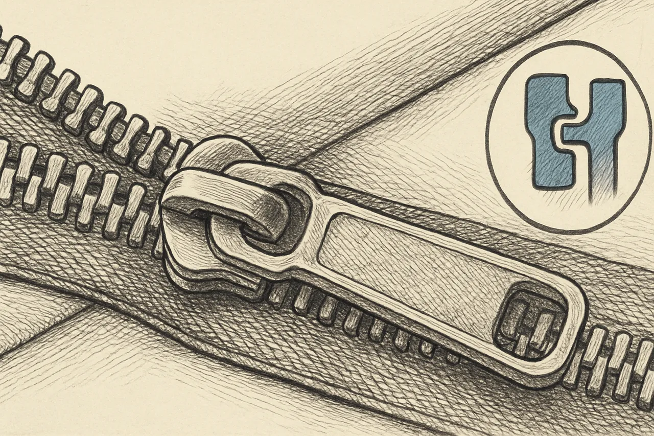
The Zipper Took Twenty Years and Three Inventors to Actually Work
The first 'clasp locker' was shown at the 1893 World's Fair and was a flop — it jammed, sprang open, and rusted. It took two more decades and a Swedish-American engineer's complete redesign to produce the interlocking-tooth zipper we use today.
Read the story →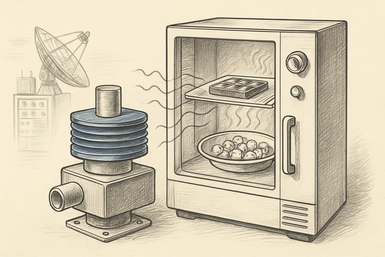
A Melted Candy Bar in His Pocket Led to the Microwave Oven
An engineer testing radar equipment noticed the chocolate bar in his pocket had turned to goo. Instead of shrugging, he aimed the magnetron at some popcorn kernels. They popped. The kitchen was never the same.
Read the story →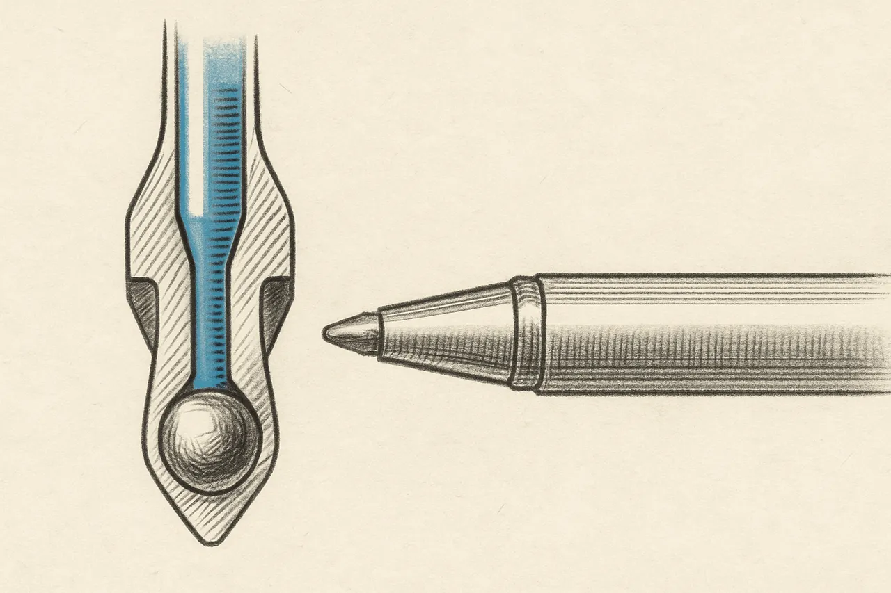
The Ballpoint Pen Took Decades and a World War to Get Right
A Hungarian newspaper editor was tired of fountain pens smudging his proofs. His fix — a tiny rotating ball fed by quick-drying ink — had been patented before and had always failed. It took him years, an escape from fascism, and an air force to make it work.
Read the story →