US 6,499,216 B1
Methods and structures for electronic probing arrays
Joseph Fjelstad,
Sunnyvale, Calif. (US)
Assigned to Tessera, Inc.,
San Jose, Calif. (US)
Filed on 24-Sep-1999, as Appl. No. Tessera, Inc.,
San Jose, Calif. (US)
Int. Cl.7A05K 3/00
U.S. Cl. 29-842
11 Claims
US 6,499,216 B1
Methods and structures for electronic probing arrays
Joseph Fjelstad,
Sunnyvale, Calif. (US)
Assigned to Tessera, Inc.,
San Jose, Calif. (US)
Filed on Sep. 24, 1999, as Appl. No. 9/405,029.
Application 09/138858 is a division of application No. 08/440665, filed on May 15, 1995, granted, now 5801441.
Application 08/440665 is a division of application No. 08/271768, filed on Jul. 07, 1994, granted, now 5518964.
Application 09/405029 is a continuation in part of application No. 09/267058, filed on Mar. 12, 1999, granted, now 6117694.
Application 09/267058 is a continuation in part of application No. 09/138858, filed on Aug. 24, 1998, granted, now 6104087.
Application 09/267058 is a continuation in part of application No. 08/989312, filed on Dec. 12, 1997, granted, now 5989936.
Application 09/405029 is a continuation in part of application No. 08/999758, filed on Nov. 26, 1997, granted, now 5983492.
Claims priority of provisional application 60/101766, filed on Sep. 25, 1998.
Claims priority of provisional application 60/077928, filed on Mar. 13, 1998.
Claims priority of provisional application 60/032828, filed on Dec. 13, 1996.
This patent is subject to a terminal disclaimer.
Int. Cl.7A05K 3/00
U.S. Cl. 298212;842
11 Claims
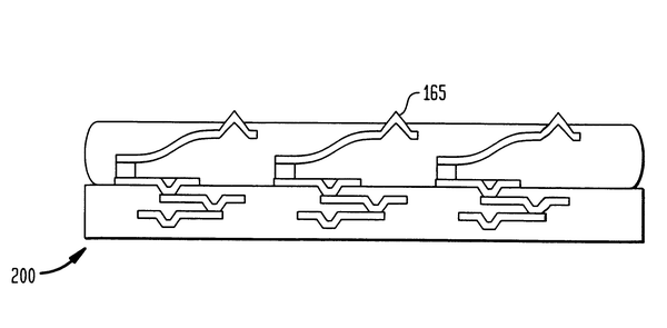
1. A method of making a probe card comprising the steps of:
(a) providing a sacrificial layer, a substrate having electrical circuits thereon and a plurality of elongated leads, each
said lead having a first end connected to said sacrificial layer, and a second end attached to said substrate and connected
to the circuits thereon, the first ends of at least some of said leads being physically connected to the first ends of others
of said leads by said sacrificial layer;
(b) moving said substrate and said sacrificial layer away from one another so as to bend the second ends of said leads away
from said sacrificial layer while leaving the first ends of said leads in position on said sacrificial layer; and
(c) injecting a flowable material around said leads and curing said flowable material to form a dielectric encapsulant layer
surrounding said leads; and
(d) at least partially removing said sacrificial layer so as to leave terminals at said first ends of said leads movable with
respect to said substrate.